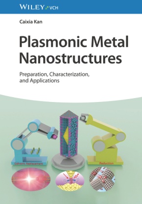
Plasmonic Metal Nanostructures - Preparation, Characterization, and Applications
| Verlag | Wiley-VCH |
| Auflage | 2024 |
| Seiten | 464 |
| Format | 17,6 x 3,3 x 25,3 cm |
| Gewicht | 1028 g |
| Artikeltyp | Englisches Buch |
| ISBN-10 | 3527351744 |
| EAN | 9783527351749 |
| Bestell-Nr | 52735174A |
This book focuses on plasmonic nanostructures and their applications, for instance, in catalyis, sensing, spectroscopy, thin-film analysis and optoelectronics.
Inhaltsverzeichnis:
PART I INTRODUCTION OF PLASMONICS
1 INTRODUCTION FOR THIS BOOK
1.1 Human beings never stop exploring light
1.2 Charming metal color
1.3 Natural development of plasmonics
1.4 About this book
PART II FUNDAMENTAL AND LATEST DEVELOPMENT IN THE PLASMONICS
2 THEORETICAL BACKGROUNDS OF PLASMONICS
2.1 Introduction
2.2 Drude model for free electron gas
2.3 Dielectric function of the free electron gas
2.4 Surface plasmon polaritons
2.5 Plasmon at metal-vacuum interface
2.6 Excitation and detection of SPP
2.7 Surface plasmon effects
2.8 Summary of this chapter
3 FUNDAMENTAL AND DIELECTRONIC MODIFICATION OF PLASMONIC NANOSTRUCTURES
3.1 Introduction
3.2 Drude-Lorentz model of metal nanoparticles
3.3 Dielectric properties of complex nanostructures
3.4 Optical property analysis of isolated nanoparticles
3.5 Numerical simulation of optical properties
3.6 Coupling nanostructure assembly with high sensitivity
3 .7 Conclusion
4 ADVANCED CHARACTERIZATIONS FOR PLASMONIC NANOSTRUCTURES
4.1 Introduction
4.2 Optical property characterization technology
4.3 Electron microscopy
4.4 Conclusion
PART III PRECISE PREPARATION OF PLASMONIC NANOSTRUCTURES
5 CORE-SHELL AND POROUS NANORODS WITH HOT SPOTS
5.1 Introduction
5.2 One-dimensional Au nanostructures
5.3 Core-shell nanostructures
5.4 Alloy Au/Ag nanorods
5.5 Porous nanorods
5.6 Yolk-shell nanostructures
5.7 Concluding remarks
6 NANOWIRES FOR CONDUCTIVE FILMS AND ELECTROMAGNETIC SHIELDING
6.1 Introduction
6.2 One-dimensional metal nanowires
6.3 Conductive films
6.4 Conclusion
7 NORMAL AND NOVEL NANOPLATES FOR UNDERSTANDING GROWTH MECHANISM
7.1 Introduction
7.2 General considerations for fcc nanoplates
7.3 Au nanoplates with novel and well-defined shapes
7.4 Summary of this chapter
8 HOLLOW AND OPEN NANOSTRUCTURES WITH ENHANCED ACTIVITY
8.1 I ntroduction
8.2 Hollow nanostructures
8.3 Open nanostructures
8.4 Optical property of Au NBP-embedded nanostructures
8.5 Conclusion and outlook
9 METAL-SEMICONDUCTOR COMPOSITE NANOSTRUCTURES
9.1 Introduction
9.2 Metal decorated semiconductor
9.3 Core-shell structure and properties modulation
9.4 Conclusion
PART IV APPLICATION EXPLORATION OF PLASMONIC NANOSTRUCTURES
10 HOT ELECTRON EFFECT ON OPTOELECTRONIC DEVICE
10.1 Introduction
10.2 Light-emitting device and modulation
10.3 Hot-electron photodetection
10.4 Conclusion
11 APPLICATIONS IN CATALYSIS AND ENERGY
11.1 Introduction
11.2 Electrocatalysis
11.3 Photocatalysis
11.4 Solar vapor generation
11.5 Conclusions and outlook
12 APPLICATIONS IN SERS AND SENSOR
12.1 Introduction
12.2 Typical SERS substrates
12.3 SERS for detection and sensor
12.4 Conclusion and outlook

